


Two SMA connectors on board for the main and the secondary (GNSS) antennas, network and status indicators, familiar 3GPP standard AT commands set, as well as the Quectel enhanced AT commands over the UART interface, USB connector for interfacing it with the software application from Quectel, are just some of the features available on the LTE IoT 2 click. A rich set of Internet protocols, industry-standard interfaces (UART, USB, SPI…) and driver support for all the major operating systems allow the Click board™ to be used in a wide range of M2M applications, such as smart metering in various industries (agriculture, gas distribution, water distribution), product tracking, and more.
How does it work?
LTE IoT 2 click is equipped with the BG96 LTE module from Quectel Wireless Solutions, which supports LTE CAT M1 and NB1 technologies, developed with IoT applications in mind. In addition, it supports EGPRS at 850/900/1800/1900 MHz, meaning that it can be used globally; it is not restricted to any region. The support for the CAT M1 and NB1 technologies and the ultra-low power consumption makes this module a perfect choice for the forthcoming 3GPP IoT technology.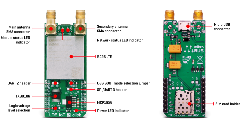
BG96 LTE module is the main component of the click board and it consists of a number of internal blocks or sections, such as the RF section, NAND flash and DDR RAM section, Power Management section, and the cellular baseband processor with the peripheral interfaces. BG96 module supports several peripheral interfaces, including USB, UART, SIM card, I2C, SPI, I2S, and GPIO interfaces. Besides the main UART interface used for exchanging AT commands with the host MCU (UART 1), there are two more auxiliary UART interfaces, one of which is shared with the SPI interface (UART 3/SPI), while the other is used for debugging purposes (UART 2). All the additional UART/SPI interfaces are available on the Click board™ in a form of unpopulated headers, with the pads clearly labeled (RX, TX for the UART debug interface header, and CLK, SDI, SDO for the SPI interface header).
The main UART interface (UART 1) supports baud rates of 9600, 19200, 38400, 57600, 115200, 230400, 460800, 921600, and 3000000 bps, with the default setting to 115200bps. This interface is used for data transmission and exchanging AT communication commands with the host MCU.
The debug UART interface (UART 2) operates at 115200bps and it is used for firmware debugging and logging the output. The UART 3 interface is multiplexed with the SPI interface and it is used to output NEMA and GNSS data sentences. It defaults to UART 3 when the module is used as the modem, but it can be also used as the SPI for the data transfer. These interfaces are not normally used, so the headers come unpopulated. If required, two standard pitch (2.54) headers can be easily soldered.
The Quectel BG96 module has to be powered by a clean and stable power supply. The voltage needed for the module to work properly is about 4V and it is derived from the 5V mikroBUS™ rail, through the MCP1826, a 1A low drop output (LDO) regulator from Microchip. Although the Quectel BG96 module is an ultra-low power device, the cellular network modules in general are notorious for their high-power consumption while actively exchange data, so 1A LDO had to be used.
Digital sections of the Quectel BG96 are supplied by 1.8V, so it is necessary to condition the incoming communication bus lines which connect the host MCU with the module. By utilizing its internal LDO regulator, the BG96 module provides the needed reference voltage for one side of the TXB0106, a 6bit bidirectional level shifter and voltage translator. The reference voltage for the other side of the TXB0106 level shifter is taken from the onboard SMD jumper, labeled as VCC SEL. This jumper is used to select between 3.3V and 5V from the mikroBUS™, depending on the used MCU type and its logic voltage level requirements.
The main UART bus of the Quectel BG96 module is connected to one side of the TXB0106 level shifter, while the other side is connected to the respective mikroBUS™ UART pins. However, the Quectel BG96 module is designed as the traditional DCE device (Data Communication Equipment) offering the full serial interface pin count, including the hardware flow control pins (CTS, RTS). These pins are routed to the mikroBUS™ CS (RTS) and the INT pin (CTS) and can be used in the MCU software if hardware flow control is needed. The RI pin is the ringing indicator, and it is routed to the mikroBUS™ PWM pin.
The STAT pin is used to signalize the status of the device. This pin is routed both to the mikroBUS™ AN pin through the level shifter, and the yellow LED labeled STAT, which is used to visually indicate the device status. The network status is indicated by the red LED labeled as TXD, located next to the STAT LED. The network status is indicated by the TXD LED, using the following pattern:
- Cyclically high for 200ms, low for 1800ms: network searching
- Cyclically high for 1800ms, low for 200ms: idle
- Cyclically high for 125ms, low for 125ms: data transfer
- Always high: voice call
The PWRKEY pin is routed to the mikroBUS™ RST pin. A LOW pulse on this pin for at least 100ms will toggle the power status of the device. If powered down, and the valid power supply voltage is present, a pulse on this pin will power up the device. The successful action will be indicated by the STAT LED and the STAT (AN) pin. If the device is already powered up, a pulse on this pin will power the module down. It is also possible to power down the module by issuing the AT+QPOWD command. Both methods are considered as safe and will let the module log off from the network and allow the firmware to save important data, before completely disconnecting the power supply. An abrupt loss of power might lead to unwanted consequences.
LTE IoT 2 click has a SMD jumper labeled as the BOOT, which is used to force the device to boot from the USB, which can be used during the firmware development or for the firmware update. During the normal operation, the USB BOOT mode is disabled.
The Micro SIM card holder on the back of the Click board™ is used to install a micro SIM card. This device cannot be used without a valid SIM card, which allows connection to the cellular network. Both 1.8V and 3V SIM card types are supported.
Specifications
| Type | GPS/GNSS,LTE IoT |
| Applications | Used for smart metering, IoT networking, remote monitoring automation and control (RMAC), and other IoT / M2M applications which rely on a cellular network connection |
| On-board modules | BGE96, a LTE CAT M1 / NB1 / EGPRS module, from Quectel; MCP1826, a 1A low drop output (LDO) regulator from Microchip; TXB0106, a 6bit bidirectional level shifter from Texas Instruments |
| Key Features | Embedded TCP/UDP/PPP stack, CAT NB and CAT M1 technologies support, enabled for all regions, aimed at M2M and IoT applications, dual SMA antenna connectors, USB connectivity, visual network and status indication, and more |
| Interface | UART,USB |
| Compatibility | mikroBUS |
| Click board size | L (57.15 x 25.4 mm) |
| Input Voltage | 3.3V or 5V |
Pinout diagram
This table shows how the pinout on LTE IoT 2 click corresponds to the pinout on the mikroBUS™ socket (the latter shown in the two middle columns).
| Notes | Pin | Pin | Notes | ||||
|---|---|---|---|---|---|---|---|
| Module status | STA | 1 | AN | PWM | 16 | RI | Ring indicator |
| Power-up module | PWK | 2 | RST | INT | 15 | CTS | UART Clear to Send |
| UART Ready to Send | RTS | 3 | CS | RX | 14 | TX | UART transmit |
| NC | 4 | SCK | TX | 13 | RX | UART receive | |
| NC | 5 | MISO | SCL | 12 | NC | ||
| NC | 6 | MOSI | SDA | 11 | NC | ||
| Power supply | 3.3V | 7 | 3.3V | 5V | 10 | 5V | Power supply |
| Ground | GND | 8 | GND | GND | 9 | GND | Ground |
Onboard settings and indicators
| Label | Name | Default | Description |
|---|---|---|---|
| PWR | PWR | - | Power LED indicator |
| LD2 | TXD | - | Network status LED indicator |
| LD3 | STAT | - | Module status LED indicator |
| JP1 | BOOT | Left | Boot operation selection: left position - BOOT mode disabled, right position - BOOT mode enabled |
| JP2 | VCC SEL | Left | Logic level voltage selection: left position 3V3, right position 5V |
Onboard connectors
| Label | Name | Description |
|---|---|---|
| CN1 | CN1 | Main antena SMA connector |
| CN2 | CN2 | Secondary antenna SMA connector |
| CN3 | - | Micro USB connector |
| J1 | - | SIM card holder |
Software support
We provide a library for the LTE IoT 2 Click on our LibStock page , as well as a demo application (example), developed using MikroElektronika compilers. The demo can run on all the main MikroElektronika development boards.
Library Description
The library carries generic command parser adopted for AT command based modules.
Generic parser
Key functions:
lteiot2_cmdSingle- Sends provided command to the modulelteiot2_setHandler- Handler assignation to the provied commandlteiot2_modulePower- Turn on module
Example description
The application is composed of three sections:
- System Initialization - Initializes all necessary GPIO pins, UART used for
the communication with LTE IOT 2 module and UART used for information logging - Application Initialization - Initializes driver, power on the module and sends few
commands for the default module configuration - Application Task Sends a message to Quectel NB-IoT test server(bit.ly/quectel-udp-server) every 5 sec.
This code snippet shows how generic parser should be properly initialized. Before initialization module must be turned on and add to that hardware flow control should be also
Commands :
Command: ATI, product information
Command: AT+IPR=115200;&W, set baudrate
Command: AT+QCFG="nbsibscramble",0, Enable scrambling
Command: AT+QCFG="band",0,0,80,1, set baud
Command: AT+QCFG="nwscanmode",3,1, Set LTE mode
Command: AT+QCFG="nwscanseq",030201,1, set priority NB1 > M1 > 2G
Command: AT+QCFG="iotopmode",1,1, select CAT-NB1
Command: AT+QCFG="servicedomain",1,1, Set PS domain
Command: AT+CGDCONT=1,"IP","internet", set APN provided
Command: AT+CFUN=1, Full functionality
Command: AT+COPS=1,2,"22001",0, set MCC and MNC provided
Command: AT+QIACT=1, activate PDP context
Command: AT+QIOPEN=1,0,"UDP","79.114.83.116",16666, create an UDP socket
Command: AT+QISENDEX=0,"48656C6C6F", Send message - Hello
void applicationInit(){// MODULE POWER ON lteiot2_hfcEnable( true ); lteiot2_modulePower( true );// MODULE INIT lteiot2_cmdSingle( &ATI[0] ); lteiot2_cmdSingle( &AT_IPR[0] ); lteiot2_cmdSingle( &AT_QCFG_1[0] ); lteiot2_cmdSingle( &AT_QCFG_2[0] ); lteiot2_cmdSingle( &AT_QCFG_3[0] ); lteiot2_cmdSingle( &AT_QCFG_4[0] ); lteiot2_cmdSingle( &AT_QCFG_5[0] ); lteiot2_cmdSingle( &AT_QCFG_6[0] ); lteiot2_cmdSingle( &AT_CGDCONT[0] ); lteiot2_cmdSingle( &AT_CFUN[0] ); lteiot2_cmdSingle( &AT_COPS[0] ); lteiot2_cmdSingle( &AT_CGATT[0] ); lteiot2_cmdSingle( &AT_CEREG[0] ); lteiot2_cmdSingle( &AT_QIACT[0] ); lteiot2_cmdSingle( &AT_QIOPEN[0] ); lteiot2_cmdSingle( &AT_QISENDEX[0] );}Alongside with the demo application timer initialization functions are provided. Note that timer is configured acording to default development system and MCUs, changing the system or MCU may require an update of timer init and timer ISR functions.
The full application code, and ready to use projects can be found on our Libstock page.
Other MikroElektronika libraries used in the example:
- String
- Conversion
Additional notes and information
Depending on the development board you are using, you may need USB UART click, USB UART 2 click or RS232 click to connect to your PC, for development systems with no UART to USB interface available on the board. The terminal available in all MikroElektronika compilers, or any other terminal application of your choice, can be used to read the message.
mikroSDK
This click board is supported with mikroSDK - MikroElektronika Software Development Kit. To ensure proper operation of mikroSDK compliant click board demo applications, mikroSDK should be downloaded from the LibStock and installed for the compiler you are using.
For more information about mikroSDK, visit the official page .
Shipping rates Australia wide and New Zealand
FAQ:
- How do I estimate shipping for my order?
- Add products in the shopping cart and head to the checkout page to estimate the shipping.
Dispatch time
Unless expressly agreed otherwise with you, we will not commence delivery of an order until we have received cleared payment of the purchase price in full.
All orders placed before 11 am AEST (Monday to Friday) will ordinarily be processed on the same day.
We will endeavour to ship the Products by the applicable time indicated on the website, but all times are indicative only. All shipping times are dispatch times only, and actual delivery dates will depend on the shipping method chosen, delivery address and delivery service provider.
Note- Please make a note during purchase if you require any item urgently. However we cannot guarantee that we will be able to comply with any request.
*Go to Australia post delivery time calculation to get various Australia post service in your area please use our shipping postcode Thomastown, 3074 as the "from" address - https://auspost.com.au/parcels-mail/delivery-times.html?ilink=tools-open-deliv-times.
We ship all products throughout mainland Australia, Tasmania and New Zealand - Including Darwin, Melbourne, Sydney, Tasmania, Adelaide, Brisbane, Perth, all metro and regional areas but do not deliver to areas in Australia where the Australia Post delivery network is not available.
Check Express shipping delivery coverage area at - http://auspost.com.au/parcels-mail/delivery-areas.html
Receipt of deliveries
Deliveries to post office boxes are not permitted where delivery is by courier. If delivery is by courier and nobody is available at the delivery address to accept delivery when delivery is attempted then the courier may either:
- leave the relevant parcel at the unattended address (the courier will do so if specified in your delivery requirements); or
- re-attempt delivery at a later time or date, in which case we may charge you an additional re-delivery fee.
Note that if a delivery is left unattended at the shipping address and is subsequently stolen then the theft is your responsibility, not ours.
Payment & Security
Your payment information is processed securely. We do not store credit card details nor have access to your credit card information.